Saturday, Oct 05 2024
What is a Pad in PCB Design and Development

By A Mystery Man Writer
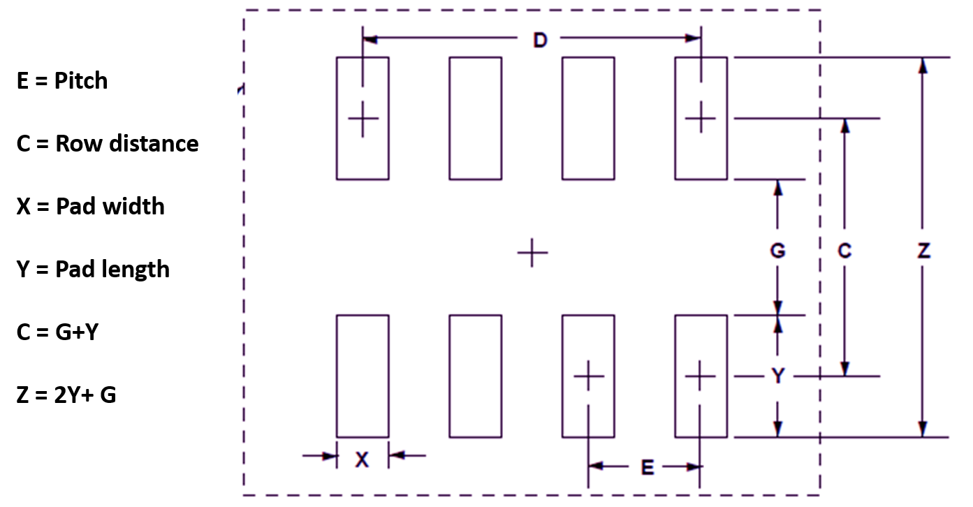
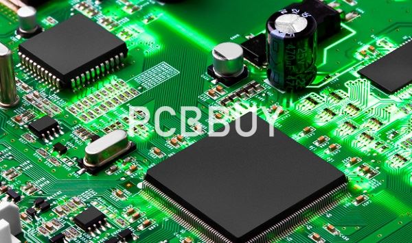
A pad is critical to PCB design as it serves as the designated surface area for electrical contact between the component and the board.
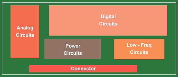
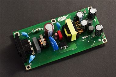
Component Placement in PCB Design & Assembly

14 Tips For PCB Design For Assembly

What is a Pad in PCB Design and Development

PCB Basic Knowledge_84
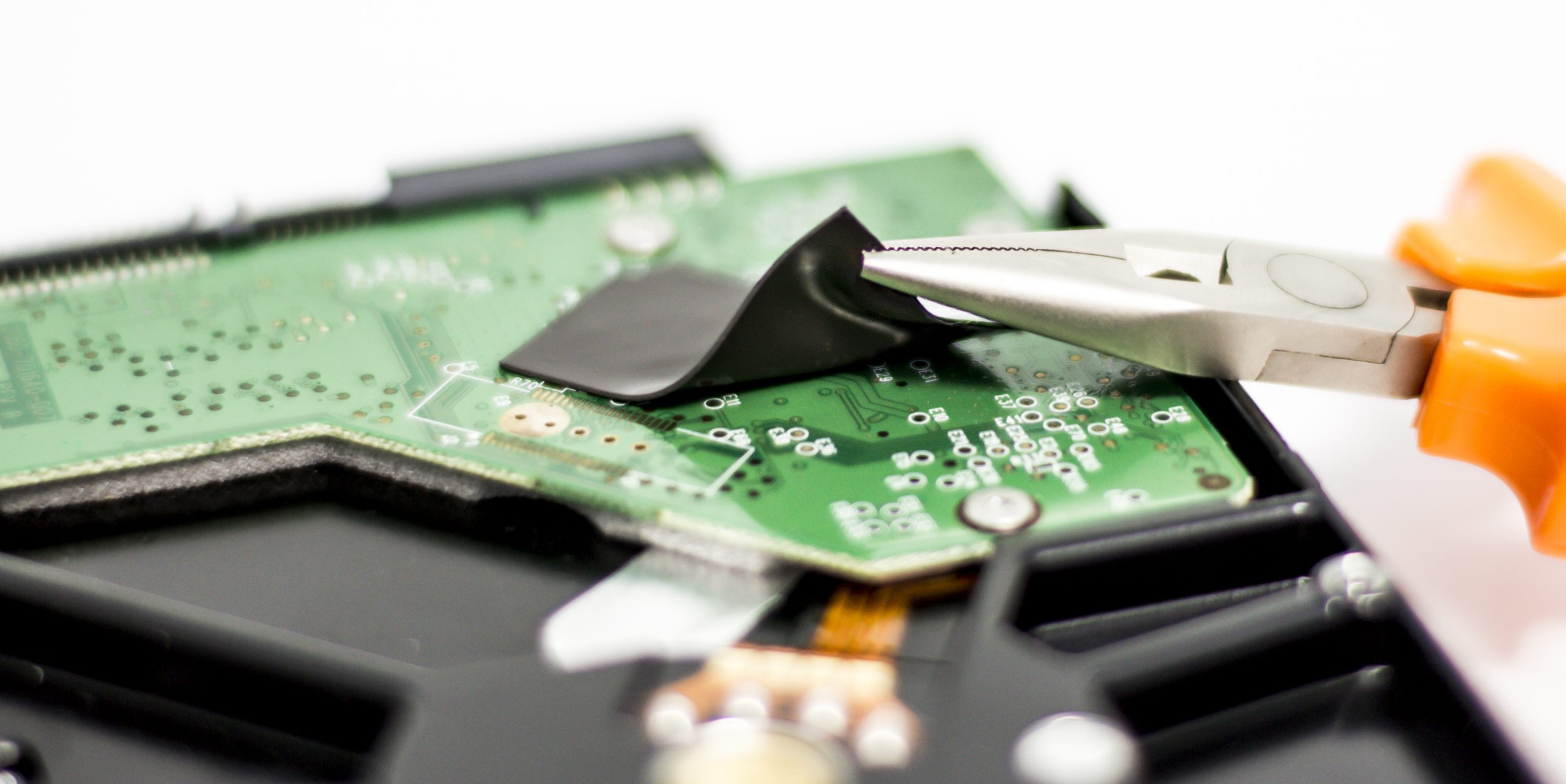
Thermal Pads in PCB Design & Manufacturing
PCB Basic Knowledge_84
What is a Pad in PCB Design and Development

Component Placement in PCB Design & Assembly
What is a Pad in PCB Design and Development
What is DRC in PCB?
PCB Basic Knowledge_100

What is a Pad in PCB Design and Development? - Absolute
Related searches
- Rifle Cheek Pad, Shotgun Cheek Pad

- OFFICIAL One Piece Mouse Pads 【 Update March 2024】
- Mouse Pad anime One Piece 90x40cm Antiderrapante - Modelo 8 - Escorrega o Preço
- Single Piece Pack Sanitary Pad at Rs 3/piece, Narela

- Ace Mall ONE Piece Portgas·D· Ace Mouse Pads with Silicone Gel Wrist Rest 3D Anime Gaming Mousepads 2Way Skin (MP1004) : : Electronics

Related searches
- Capezio Women's Professional Fishnet Tights – Ballera Dance

- AVENUE BODY | Women's Plus Size Seamless Shaper Slip - black - 18W/20W
- New Balance Printed Impact Run Light Pack Jacket - Sulpher Yellow

- Big Girls Don't Cry Anymore (@biggirlsdontcryanymore) • Instagram photos and videos
- Realistic Silicone Man Muscle Chest Abdominal Fake Muscle Suit For Cosplay


©2016-2024, reintegratieinactie.nl, Inc. or its affiliates