Scaling Bump Pitches In Advanced Packaging

By A Mystery Man Writer
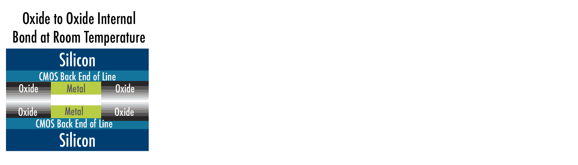
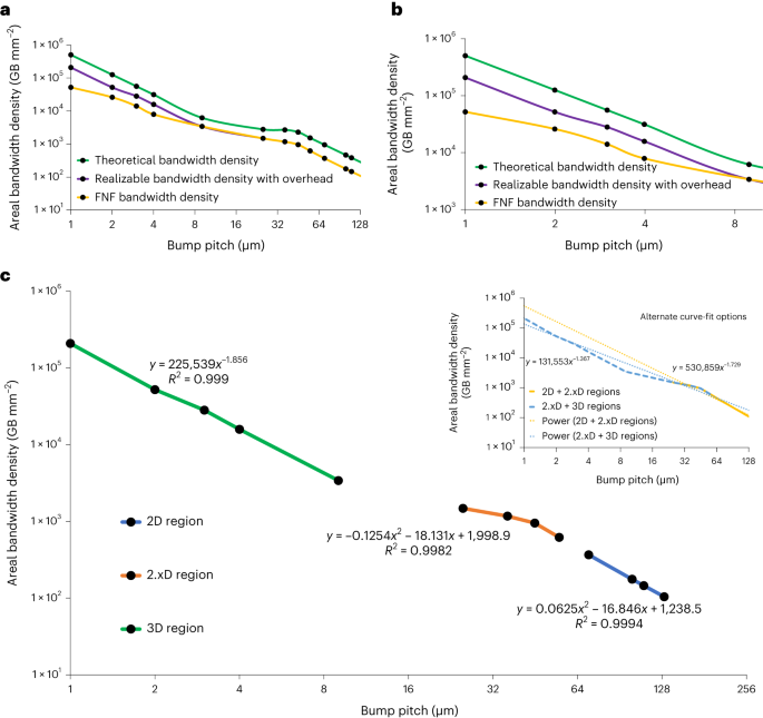
Higher density of interconnects will enable faster movement of data, but there's more than one way to achieve that.
Hybrid Bonding Basics – What is Hybrid Bonding? - Brewer Science
Advanced Packaging Part 1 – Pad Limited Designs, Breakdown Of Economic Semiconductor Scaling, Heterogeneous Compute, and Chiplets
Tighter Integration Between Process Technologies and Packaging - EE Times Europe

How chips are interconnected - PCBA Manufacturers
MicroLED: Technology Advancements Thread, Page 42

Process and Key Technology of Typical Advanced Packaging

TSMC-SoIC® - Taiwan Semiconductor Manufacturing Company Limited
High-performance, power-efficient three-dimensional system-in-package designs with universal chiplet interconnect express

Introduction to solder paste corrosion testing

Additive manufacturing of metal interconnects using microscale selective laser sintering


- 6 Pack Womens Plus Size Seamless Briefs No Show Full Coverage Panties 2X 3X

- Uma das maiores rivalidades do futebol, Boca x River será atração

- Ladies - Womens 1X - 2X - 3X & 4X Plus Size - Queen Size Clothing

- High waist Adidas Climalite leggings, great

- KOODEE LAUNCH PANIHARI VOL 2 COTTON KURTI WITH PANT DESIGN
