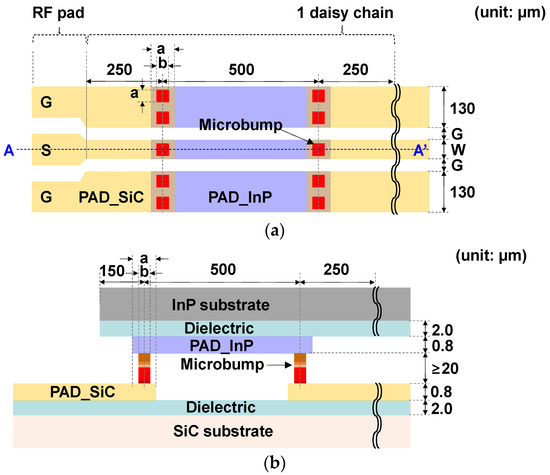
PDF] Design and Fabrication of Bond Pads for Flip-Chip Bonding of

By A Mystery Man Writer
At the University of Alberta, the Imaging Science Lab aims to develop vertically-integrated (VI) CMOS image sensors with capabilities that exceed those of conventional CMOS image sensors. VI-CMOS image sensors are examples of 3D electronics because they consist of photodetectors that are placed in a layer above standard CMOS circuits. Although metal lines commonly pass over transistors in CMOS image sensors, a distinguishing characteristic of VI-CMOS image sensors is the layering of semiconductor devices. The main advantage of vertical integration is that the different layers may be fabricated using different processes, each one optimized to best suit the type of devices it contains.

Global Flip Chip Technology Market Size And Forecast 2023-2030
Soft ionic liquid multi-point touch sensor - RSC Advances (RSC

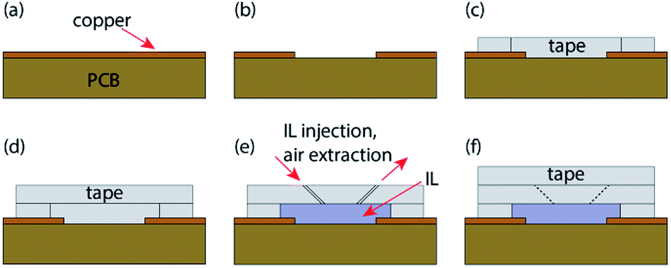
IC Assembly, PDF, Epoxy
Micromachines, Free Full-Text

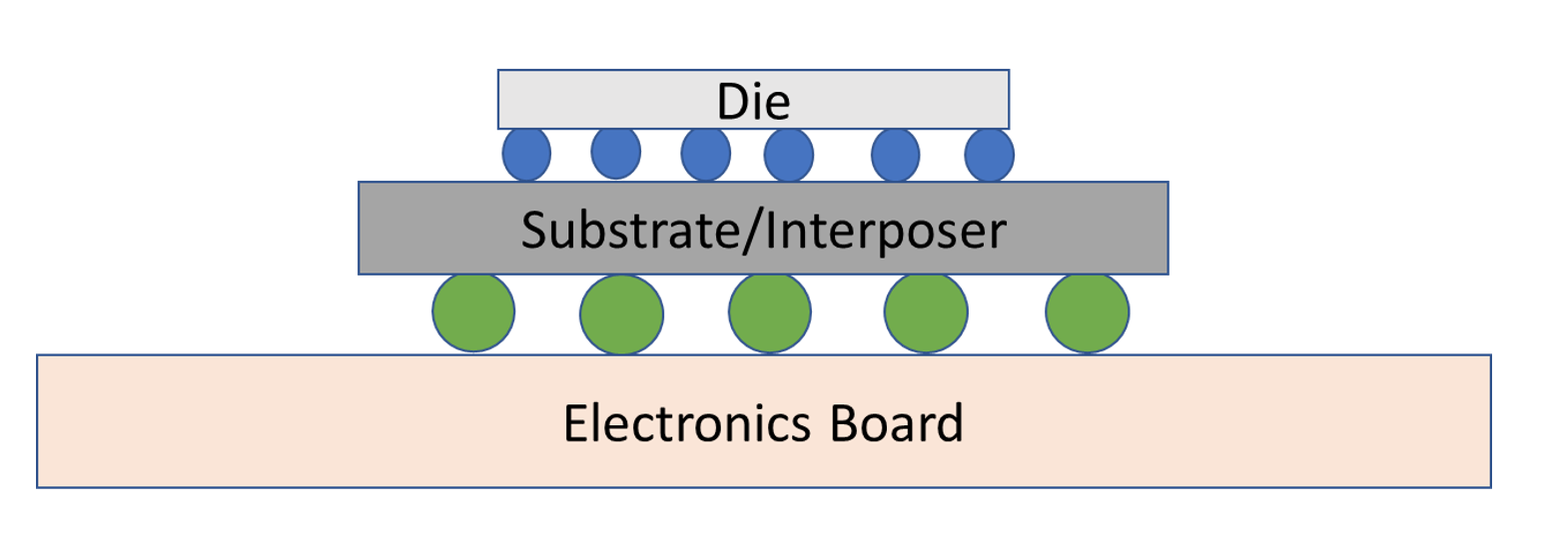
Flip Chip technology
Wire Bonding, Advanced PCB Design Blog
Challenges Grow For Creating Smaller Bumps For Flip Chips

Digital Design

Bonding process of the ACF flip chip package; (a) before bonding

- Long Sweaters for Women to Wear with Leggings Casual Knitted Pullover Mini Dress Women Open Sweater (Blue, S) : Clothing, Shoes & Jewelry

- HALTEC Truck Valve Extension: Valve Extensions, Straight Grip Tire Valve Extenders, Round, Silver
- Mais de 50 milhões de horas. Essa foi a magnitude alcançada pelo filme “Depois do Universo”, uma produção nacional da Netflix, mu
- Sunkissed Skort Dress

- Seamless Jumpsuit Sports Wear Beige